Dual 3-ADC PXI Express Hybrid Peripheral Module
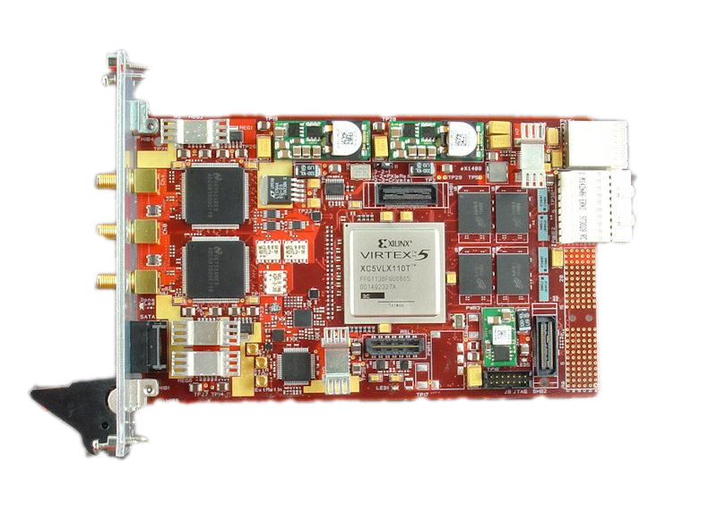 The SMT702 is a PXI Express (opt. Hybrid) Peripheral Module (3U), which integrates two fast 8-bit ADCs, a clock circuitry, 2 banks of 1GByte DDR2 Memory each and a Xilinx Virtex5 FPGA, under the 3U format.
The PXIe specification integrates PCI Express signalling into the PXI standard for more backplane bandwidth. It also enhances PXI timing and synchronisation features by incorporating a 100MHz differential reference clock and triggers. The SMT702 can also integrate the standard 32-bit PXI signalling as an option.
Both ADC chips are identical and can produce 3 Giga-samples per second each, with an 8-bit resolution. The manufacturer is National Semiconductor and the part number is ADC083000. Analog-to-Digital converters are clocked by circuitry based on a PLL coupled with a VCO in order to generate a low-jitter signal. The ADC083000 is capable to achieve 7 bits of ENOB, 44dBs of SNR and 54dBs of SFDR. The full bandwidth is 3GHz. Each ADC integrates settings such as offset and scale factor, which makes the pair of ADC suitable to be combined together in order to make a 6GSPS single Analog to Digital converter. This will be subject to a specific application note.
 An on-board PLL+VCO chip ensure a stable fixed sampling frequency (maximum rate), in order for the board to be used as digitiser without the need of external clock signal. The PLL will be able to lock the VCO either on the on-board 100MHz reference or the 100MHz PXI express reference (or 10MHz PXI reference depending on option) or on an external reference signal. The sampling clock for the converters can be either coming from the PLL+VCO chip or from an external source. The chip used is a National Semiconductor part: LMX2531LQ1500. The reference clock selected is also output on a connector in order to pass it to an other module.
The Virtex5 FPGA is responsible for controlling all interfaces, including PXI (32-bit) and PXIe (8 lanes allocated – depending on PXIe chassis, 4 or 8 lanes would be used), as well as routing samples. On the SMT702 the FPGA is an XC5VFX70T, which is footprint compatible with XC5VLX85T,XC5VLX50T, XC5VLX110T. Note that all Virtex5s connect PXIe and only the XC5VLX110T will allow the full 32-bit PXI format.
Two 1GB DDR2 memory banks are accessible by the FPGA in order to store data on the fly.
An SHB connector is available (XC5VLX110T only) in order to transfer data/samples to an other Sundance module.
All analog connectors on the front panel are SMA.
Application Note – Multiple SMT702 System
Application Note – Multiple SMT702 System
Application note SMT702_SMT712 System
AppNote_FFT_SMT702 SMT702 Product Specification
s702