We have designed a new I/O board for a customer’s project using SolidWorks PCB to carry out the placement and routing. This is new for us as we would normally use Cadstar for this part of the procedure. The advantage of the new approach is that it provides a 3D visualisation of the whole design prior to final production, making the placement and routing of components and connectors on the PCB less problematic.
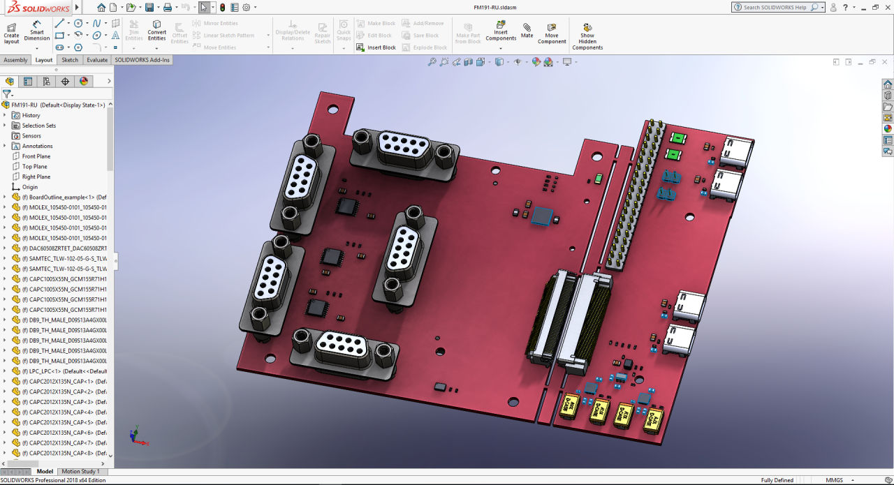
PCB physical design in SolidWorks.
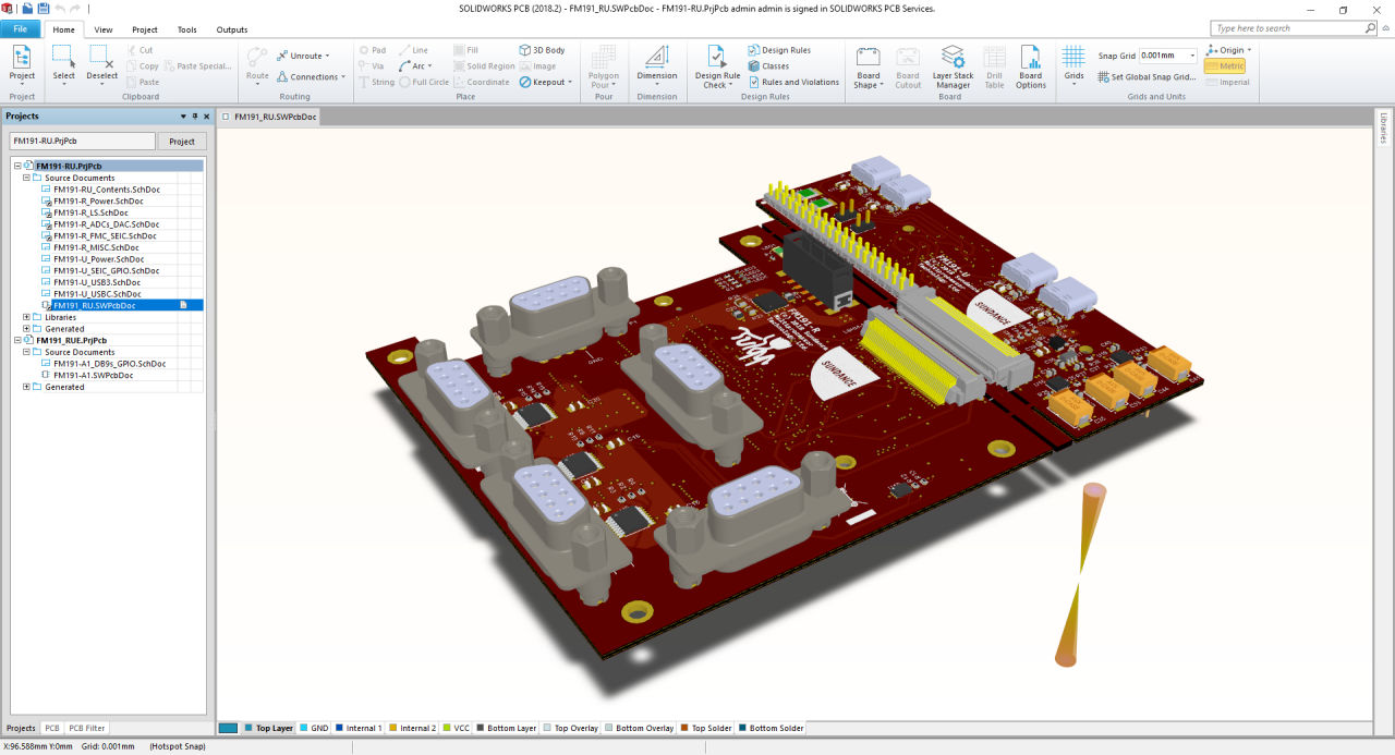
PCB design pulled from SolidWorks into SolidWorks PCB and then populated and routed .
Timoteo, the engineer that carried this out, had this to say about the process:
I had to design an FMC board compatible with the EMC2-DP, that would provide the I/Os required by our customer. Using SolidWorks PCB, I learnt how to create schematics, and import that information into a PCB design. As this board had a lot of I/Os, including differential pairs, I had to organise all of the components correctly and distribute the routing of them using 6 layers.
SolidWorks PCB is based on Altium, which is a new package for all of us here at Sundance. Despite this I’ve managed to determine the outline of a PCB from a 3D model in SolidWorks, or push/pull information between the mechanical and electronics design tools.
It has been an interesting experience, as it’s not only about creating a board in a software tool, but being part of a production chain, where I have to provide a parts list with available components in the market, and take into account the limitations in terms of parameters (widths, shapes) depending on the PCB provider chosen.
Another benefit of designing with SolidWorks PCB is that the 3D visualisation of the finished board can be used to create assemblies with other boards/systems and also create bespoke cases and enclosures for them.
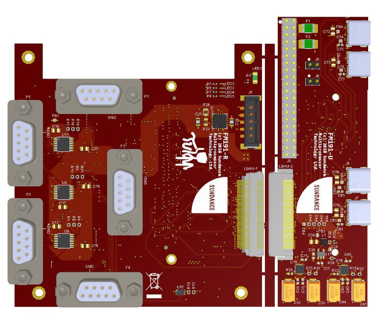
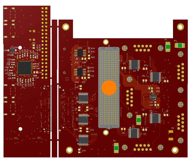
The finished designs:
.