 Dual ADC/ DAC module
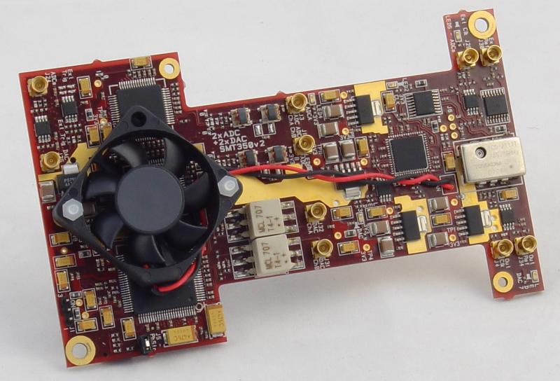
The SMT350 is a single width expansion TIM that plugs onto the SLB base module SMT368 (Virtex4 FPGA) and incorporates 2 Texas Instrument Analog-to-Digital Converters (ADS5500) and one Texas Instrument dual-channel Digital-to-Analog Converter (DAC5686). The SMT350 implements a comprehensive clock circuitry based on a CDCM7005 chip that allows synchronisation among the converters and cascading modules for multiple receiver or transmitter systems as well as the use of external clocks. It provides a complete conversion solution and stands as a platform that can be part of a transmit/receive base station. External Triggers are also available.
ADCs are 14-bit and can sample at up to 125 MHz. The DAC has a resolution of 16 bits and is able to update outputs at up to 500MHz. All converters are 3.3-Volt.
 The Xilinx FPGA (Virtex 4) on the base module is responsible for handling data going/coming to/from one of the following destination/source: TI converters, Comport (TIM-40 standard), Sundance High-speed Bus (SHB), ZBTRAM Memory. These interfaces are compatible with a wide range of Sundance’s modules.
Features
- Two 14-bit ADCs (ADS5500 – TI) sampling at up to 125 MHz
- One 16-bit, 2x-16x interpolating dual channel DAC (DAC5686 – TI)
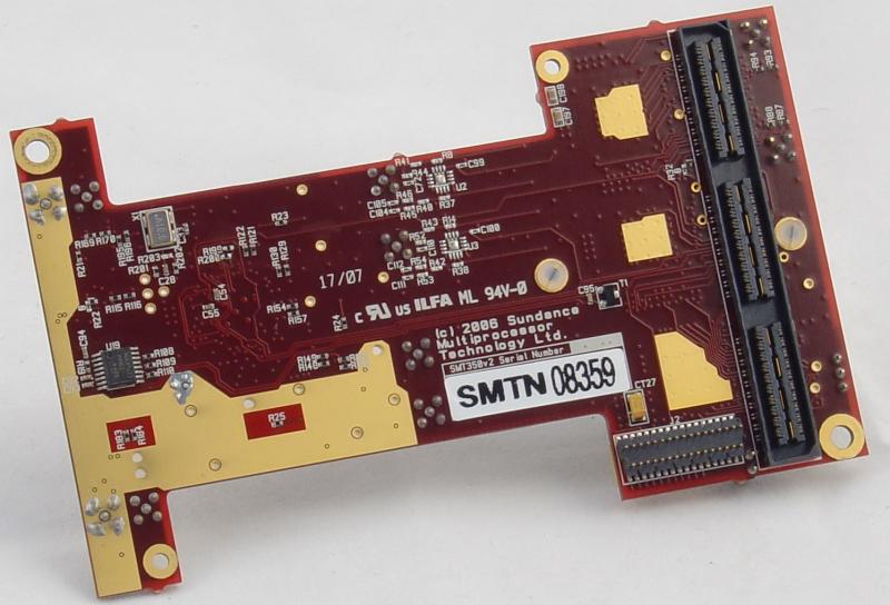
- One SLB connector to link the SMT350 with an SMT368
- Single width expansion module (mezzanine module)
- On-board low-jitter clock synchronizer
- One external clock and Two triggers via MMCX connectors (Huber Suhner)
- External reference clock for synchronising and cascading modules
- Analogue Inputs/Outputs via MMCX (Huber Suhner) connectors for connection to 50-Ohm sources/loads
Benefits
The SMT350 can be used for Intermediate-Frequency (IF) sampling architectures, cellular base stations such as CDMA or TDMA, baseband I/Q systems, wireless communication systems, Instrumentation, etc.
SMT350_Technical_Specification
SMT350v2_Performance SMT350_User_Manual